Tech notes
Curled Microelectromechanical Switch
Curling the electrode of a microswitch virtually eliminates sticking and dielectric charging, leading to more consistent operation and longer lifetimes.
Microelectromechanical switches (MEMS) are active components in most electronic equipment. Radio frequency (RF) MEMS are used in wireless personal communication devices, satellite communication, and phased array antennas. MEMS are ideal for these applications because of their low weight, small surface area, low volume, high isolation, large frequency range, linearity, and low power consumption.
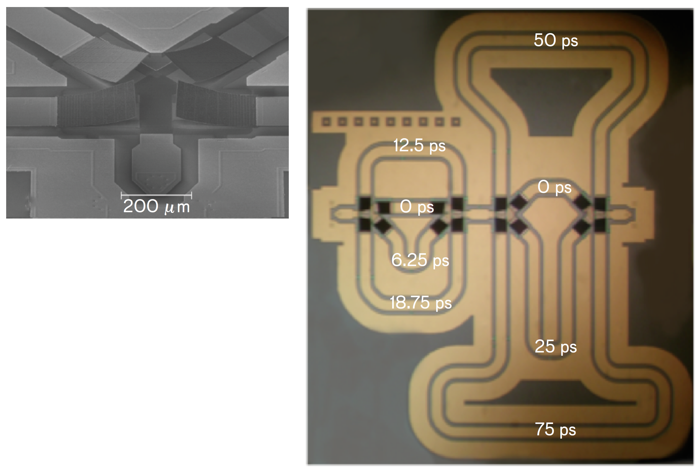 CMEMS can be combined to create a multiswitch "pad." Shown above is a four-switch component (without protective caps) that, when combined with three other such components as seen on the right, can produce a true time-delay circuit of 16 possible outcomes.
While MEMS have many positive attributes, reliability has been a challenge with the charged dielectric; stiction and deformation are two primary cause of failure. In addition, contact welding and contamination of the switch by foreign debris are also problematic. These problems are partly due to the design of the MEMS. In traditional MEMS, the "upper" contact electrode is bridged or flat-cantilevered over the "lower" electrode; there is no significant separation between the electrodes in the off state.
The Curled Microelectromechanical Switch (CMEMS) is a breakthrough technology in on-chip switching design. The switch is a highly flexible and robust curled membrane structure protected by a single-crystal hermetic cover. The curl, corrugation, and cover ensure that the sticking, dielectric charging, and contamination issues associated with traditional MEMS switches are virtually eliminated.
CMEMS Technology
The innovative design of the CMEMS device includes the curled electrode, itself a corrugated trilayered aluminum-silica electrode, and the single-crystal silicon cover. At the heart of CMEMS are the three electrodes. The curled electrode is specially designed with a built-in strain and corrugation to make it roll up and down uniformly. There are two fixed flat electrodes on the substrate. The capacitive (on/off contact) electrode is surrounded on three sides by a pull-down electrode. A voltage, usually a low-frequency squarewave signal, is applied between the curled electrode and the pull down electrode, creating a force that flattens the curled membrane against the pull down and capacitive electrodes on the substrate ("on" state). A significantly lower voltage is applied between the capacitive plates where there are fewer corrugations. The movement of the curled electrode causes a large change in the capacitance between the curled and capacitive electrode. This change in capacitance, from off to on states, provides the switching action for the RF signal.
Trilayered Aluminum Silica Structure
The robust trilayer structure, aluminum sandwiched between two silica layers, balances the stress in the curled electrode and provides high conductivity. The unique trilayer structure prevents elastic deformation, plastic deformation, fracture, and fatigue, all of which are common difficulties with traditional MEMS switches.
Corrugated Design
Corrugations were designed into the switch to induce the proper curl direction (when combined with the intrinsic strain induced by the trilayering). The corrugated structure has a second function—to reduce the field strength when the electrode is rolled out and in "contact" with the pull-down electrode.
Single-Crystal Silicon Cover
MEMS switches have historically had to deal with contamination. The CMEMS single-crystal silicon cover is strong and is the ultimate gas diffusion barrier protecting the device from contamination. It is designed to protect each switch but at the same time, it enhances the RF properties of the switch. The cover, itself an intrinsic component of the CMEMS circuit, provides for a very low RF loss and tight confinement of the RF signal.
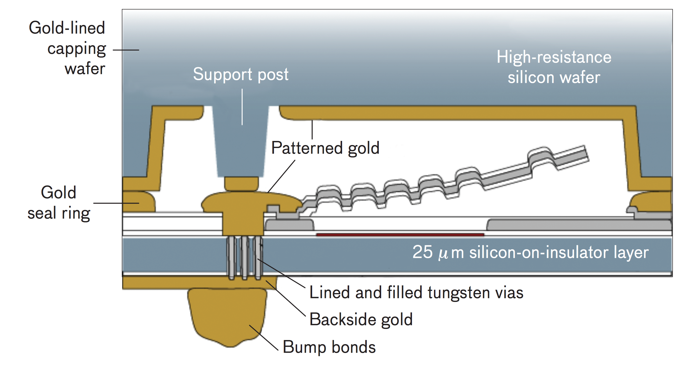 The trilayer membrane has an internal strain that makes its natural state a highly curled arch, well-separated from the capacitive electrode. This separation results in a very high capacitive difference between on and off states, thus eliminating any potential for stiction or leakage in the off state. The single-crystal cover is an integral part of the RF electronics and provides all connections to the switch in the same footprint size, eliminating bulky contacts. The gold ring is thermocompressed to form the hermetic seal. The interior chamber is RF isolated, making it an ideal RF waveguide.
Benefits of CMEMS
CMEMS is designed especially for switching alternating-current RF signals above 1 GHz. CMEMS functions over a broad bandwidth, with high linearity, with lower loss—a critical parameter for cell phones that rely on battery power—and with the added advantage of small size and weight. One application for which size, weight, and bandwidth are critical is in the RF switching stations found in cell phone ground stations and in satellites. The low loss and immunity from drift are of course critical also in these applications.
The principal advantage of a switch having a moving metal electrode is the large impedance change that can be achieved. The unique character of CMEMS is the curled electrode that gives by far the largest impedance change of any MEMS or other on-chip switch as it moves from the open curled state to the closed state. The uniqueness of the CMEMS design
- Provides a high-power capability for numerous device applications
- Can carry more information because of its wide bandwidth capability
- Has a small package dimension, reducing circuit size to much smaller than RF wavelengths, and allowing for true phase shifting
Benefits of WACS
The WACS technique enables the measurement of concentrations of specified target gases within the atmosphere at longer ranges than those achieved by other active optical techniques, while using a much lower-power laser source for a given range. Additionally, WACS is capable of at least five times the absolute sensitivity of other sensors at the longest ranges because of its ability to measure and remove the effects of spectral drift, atmospheric contaminants, and atmospheric scintillation.
Because WACS can detect and localize even small quantities of a gas, it can identify, for example, natural gas pipeline leaks as low as 100 g/hour. WACS can collect such low concentrations of gases in fractions of a second. Placed on a mobile platform, WACS can achieve area coverage rates of 100–1000 km2/hour (for wide-area search, rates of >100 km2/hour are ideal).
The WACS system has several advantages over other long-range spectrometers:
- The instantaneous (per-pulse) measurement of gas concentrations eliminates atmospheric scintillation noise.
- Sensitivity degrades much more slowly with range because of active clutter compensation.
- Low laser power and stability requirements reduce system cost.
- Separation of the transmitter and receiver enables the localization of gas releases without directly illuminating the release location.
- Is stable over wide temperature ranges, to permit usage in extreme environmental conditions
- Is extremely reliable—the number of cycles before failure opens up many potential applications
- Eliminates the sticking problem inherent in other MEMS devices
- Has a closed loss less than 0.1 dB and open isolation greater than 20 dB over a frequency band of 5 to 40 GHz (for a single packaged switch)—the best-reported results for any MEMS switch over this frequency band.
Applications
RF MEMS switches are ideally suited for use in wireless personal communication devices, satellite communication, and phased array antennas. The CMEMS design not only dramatically reduces the failure modes typical to other MEMS devices but significantly improves the capabilities as well.
The prime example of an application for CMEMS is a true time-delay circuit for a phased array antenna. For the first time, a MEMS switch is compact, low loss, and reliable enough to eliminate the need for the current multiplicity of amplifiers. By using a low-loss phase shifter at each pixel, a single power source can be split between all pixels. Low-cost arrays could make possible their use on vehicles and as fixed sensors. In the future, we may have satellite communication via car roof antennas and radars around cars and homes.
Posted November 2014
top of page