Publications
Lab Notes
| ASTRONOMY Vision Correction |
Posted November 2010 |
Two projects should help astronomers see further across the universe. |
|
The history of the universe is laid out across the sky, with the earliest events—the birth of stars and formation of galaxies—the furthest away, at roughly 11 billion lightyears. To study the oldest, dimmest parts of the cosmos, astronomers are building larger, more sensitive telescopes. Lincoln Laboratory is developing technology that could help the planned next generation of ground-based telescopes see stars no human has seen before.
The Laboratory's Advanced Imaging Technology (AIT) Group is working on two instruments to aid the Thirty-Meter Telescope (TMT), an instrument that should be built on Mauna Kea, Hawaii, within the next decade. With a 30-meter-diameter mirror, made up of 492 individual segments, the TMT vastly increases the light-collection area, and therefore the sensitivity, over that of the 8- and 10-meter telescopes in use today. The AIT Group, in collaboration with Sean Adkins of the W.M. Keck Observatory in Hawaii, is working on a charge-coupled-device (CCD) sensor that will let this telescope see more clearly.
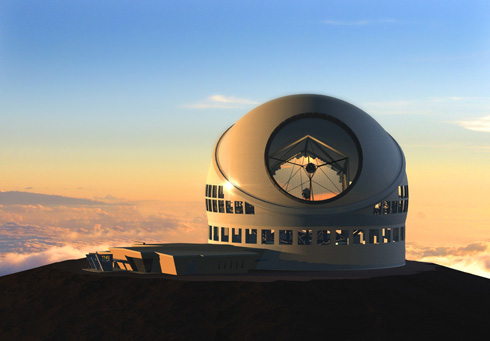 The CCDs under development at Lincoln Laboratory will be used in the Thirty-Meter Telescope, shown in an artists conception. (Image courtesy of TMT Observatory Corporation. Rendering by Todd Mason.)
The TMT will rely on adaptive optics to overcome distortions caused by turbulence in the Earth's atmosphere. Adaptive-optics systems, like the one in use at the 10-meter Keck telescope, fire a laser beam into the thin layer of sodium located about 90 kilometers above the ground, causing the sodium to fluoresce and produce a glow that serves as a "guide star." The specialized CCD measures wavefront distortions in the light coming back from the sodium layer and uses these measurements to tell a series of actuators how to push and pull on the telescope's mirror to compensate for the atmospheric distortions. Fluctuations in the atmosphere happen on a time scale of about 10 milliseconds, so all the measurement and correction has to be done within that time.
"It's not very poetic," says materials scientist James Gregory, assistant leader of the AIT Group, "but we're taking the twinkle out of the stars."
To measure the shape of the wavefront across the area of the telescope aperture, the CCD is placed behind an array of microlenses. These microlenses divide the sensing device into "subapertures," each comprising multiple pixels. Each microlens focuses the light from the guide star into a spot, and the position of the spot on the CCD pixels is used to compute the tilt of the wavefront at the corresponding point in the telescope aperture.
The trouble with using a laser guide star with the TMT is that the sodium layer is generally 15 to 20 km thick. If the laser beam is sent straight up from the center of the telescope, then someone standing right next to the laser could look up and see a spot of light. But an observer standing further out toward the edge of the telescope would see the side of a column of light going through the sodium layer—that is, the spot now appears as a streak. While a spot would illuminate only a handful of pixels on a CCD sensor, the streak will illuminate many of them. Because each pixel will inevitably produce a certain amount of electronic noise in the act of reading out the data, a higher number of pixels leads to a lower signal-to-noise ratio.
"You don't have a lot of photons coming back to work with in adaptive optics, so signal-to-noise is everything," explains AIT Group leader Robert Reich.
To limit the number of pixels involved, Brian Aull, Barry Burke, Bradley Felton, and Kay Johnson of the AIT Group are designing a new type of CCD sensor, conceived in collaboration with Sean Adkins of Keck Observatory, Jim Beletic of Teledyne Imaging Systems, and Jerry Nelson of the Center for Adaptive Optics at the University of California, Santa Cruz. Instead of the standard contiguous rectilinear array of pixels, they are making what they call a polar coordinate detector. Each subaperture has its own miniature CCD, with just enough pixels to image the streak of light. Furthermore, each CCD is oriented to form columns of pixels radiating out from the center of the sensor to the edge, like lines of longitude radiating out from the North Pole in a map looking down on the top of the Earth. Because the CCD columns are aligned along the streak of laser light, the CCD can be narrow in the direction perpendicular to the streak. This scheme minimizes the number of pixels needed behind each microlens; as a result, the sensor has fewer pixels to read. Because signal-to-noise ratio varies by the square root of the number of pixels read out, cutting the pixel count in half is equivalent to making the signal 40 percent stronger.
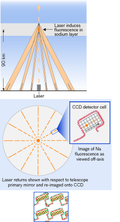 The CAD layout of CCD cells at the bottom shows interconnecting readout registers, which transport the charge to the periphery of the CCD for conversion to video signals.
6 × 15 formation.
Transferring the signal from the polar imager off chip proved to be challenging. A rectilinear imager design would have simple wiring and selection logic circuitry at each pixel array associated with a microlens. The addressing and multiplexing of the signal off chip would be straightforward. But for the polar-imager design, in which sizes and directions vary, such a scheme would have been a nightmare of complexity, Reich says. Instead, his team, following a suggestion by Sean Adkins, figured out how to pipeline the readout registers of the pixels in series and load all the data from behind each microlens into the register so there were no gaps.
The design work is well under way, Reich says, and the team should be able to have a one-quarter chip fabricated early next year. If that device works, they'll build a full chip. Once they're satisfied, they can pass the CCD on to the team building the TMT.
"We are definitely planning on using it and factoring it into our design," says Brent Ellerbroek, group leader for adaptive optics on the TMT project, which is a partnership of the University of California, California Institute of Technology, and the Association of Canadian Universities for Research in Astronomy. "It's a very important innovation that simplified the system and improves the performance in a lot of ways."
The second instrument the team is developing is not part of the adaptive-optics system, but will take advantage of the tiny number of photons collected by the telescope to make better pictures of distant galaxies. Aull and team member Daniel Schuette, along with Felton, and in collaboration with Donald Figer of the Rochester Institute of Technology, are designing a photon-counting imager based on Geiger-mode avalanche photodiodes. This imager will improve the sensitivity of the telescope so it can see dimmer objects at a given distance, or find bright objects further away.
The imager grows out of the team's work using similar photodetectors in laser detection and ranging (ladar) systems. A Geiger-mode avalanche photodiode is put into an unstable state by the application of a high voltage, typically about 30 volts. A photon that strikes the device creates a pair of charge carriers—an electron and a hole. When one of these carriers is drawn into and accelerated by the diode's high-electric-field region, it gains enough energy to create new electron-hole pairs each time it collides with atoms in the semiconductor lattice. The electrons and holes released by these collisions are then themselves accelerated by the high field, creating a cascade of electric current. The net result: capture of a single photon triggers an easy-to-detect burst of electrons. Ladar systems use these photodiodes to detect how long it takes for a photon leaving the laser to bounce off an object and return, thereby allowing calculation of the distance to objects. Compiling a large number of such range readings yields a three-dimensional picture of a scene.
Astronomers are not as interested in when photons reach the telescope as they are in accurately measuring the total number of photons that the telescope sees. Analog detectors generate some noise every time a pixel is read out, making it difficult to see faint objects spread over many pixels. In a photon counting imager, however, observation of each photon is recorded as a bit in custom all-digital circuitry that is directly linked to the photodiode array. Consequently, there is no readout noise—a signal is produced for each photon that is captured, and no signal is produced if there's no photon. "You're essentially at the limit of how good you can be," Reich says. "It's as quiet as you can get. You're counting every photon."
 |
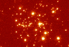 |
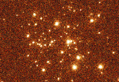
These simulated images of the Arches Cluster near the Galactic Center are based on Keck/LGSAO data and are courtesy of the Rochester Institute of Technology. The image on the left has read noise comparable to that in detectors currently planned for TMT. The image on the right has zero read noise. |
|
Reich says he expects within the next two years to build an array of avalanche photodiodes for the TMT by using silicon, but that the project may ultimately move to a different Lincoln Laboratory group that works with compound semiconductors rather than silicon. The reason for this shift is that astronomers need detectors to work at wavelengths between 1 and 2.4 micrometers, where materials such as indium-gallium-arsenide are more sensitive (light that originates from stars a vast distance away is red-shifted from the visible into the infrared by the expansion of the universe). Ellerbroek points out that, because longer wavelengths are less disturbed as they pass through the atmosphere, adaptive optics work better in the infrared, where astronomers can get near-diffraction-limited performance.
But compound semiconductor materials present a number of challenges that make them, currently, poorly suited for an astronomy imager. A team lead by Simon Verghese, assistant leader of the Laboratory's Electro-optical Materials and Devices Group, is working to address these issues. For now, silicon is better understood and better developed for this sort of detector. Says Reich, "we'll be the pathfinders."