PUBLICATIONS
Lab Notes
| SEMICONDUCTORS | Published in the Lincoln Laboratory Journal, vol. 17, no. 1, November 2007 |
Small Packages |
|
If engineers could pack circuits made of normally incompatible materials together on the same silicon chip, it could lead to lower-cost radar modules, less power-hungry cell phones or other wireless devices, and smaller, cheaper radio frequency identification (RFID) tags. One Lincoln Laboratory researcher thinks he has come up with a way to integrate transistors made using complementary metal oxide semiconductor (CMOS) processes with other devices built from compound semiconductors, such as the III-V materials gallium arsenide or indium phosphide.
"CMOS is very good, especially for digital-logic, low-power applications, whereas a lot of III-V devices can have superior transistor speed and higher gain,” says Jeremy Muldavin, an electrical engineer in the Laboratory’s Advanced Silicon Technology group. “You’d like to be able to pick and choose which transistor technology you use for which function.”
Muldavin has come up with a packaging scheme that he says will let engineers pick the very best materials for every application, perhaps using silicon to provide digital processing and III-V devices for amplification or radio frequency transmission. Such flexibility could lead to power efficiencies and smaller overall devices. He has developed a way to isolate individual transistors so that they can be placed in the most convenient location without creating electrical interference with neighboring transistors. The packaging makes it much more practical to integrate CMOS and III-V devices on the same silicon chip, which until now has been a difficult challenge.
A key problem to overcome is electromagnetic interference. An active component, such as a field-effect transistor, gives off an electromagnetic field and needs to be placed far enough away from similar components that the two fields won’t interfere with each other. That limits how many active components a chip can have and how small the chip can get. “You could have a huge number of things in that area if you could find a way to isolate them,” Muldavin says.
He achieves that isolation by using micromachining techniques to build cavities coated with a conductive metal, essentially creating little cans into which he can place active components. That allows him to add a few dozen III-V transistors made of different compound semiconductors onto a chip without wasted space and without electromagnetic interference. The design, he says, is good for systems with a fairly high density of CMOS devices and a low number of III-V devices.
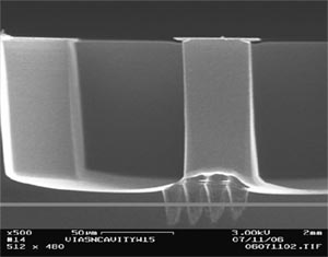
He starts with a layer of bulk silicon, about 100 μm thick, on top of an insulator, and etches into this silicon a series of small, flat-bottomed wells about 90 μm deep. He then makes another layer with its own series of wells that he places of top of the first layer. He coats the surfaces of each piece with a conductive metal, preferably gold, although copper is also a possibility. He places the active component within the wells, then bonds the two pieces together, separated by a thin layer, perhaps 10 μm thick, of high-resistivity silicon. Now each component sits in its own little cavity, completely surrounded by metal. In certain spots, a tiny via pokes all the way through the silicon to the insulator, providing a conduit for the electrical connection. The layers of metal create what is essentially a coaxial transmission line, carrying power to the components with little insertion loss while isolating the electromagnetic fields. The bulk silicon helps the III-V devices operate better by carrying away the excess heat they generate.
One previous approach some engineers have taken to mix and match dissimilar materials is to grow the III-V crystals on the same chip where the CMOS devices are built. Unfortunately, the lattice structures of the III-V crystals don’t match very well with those of the silicon crystals, limiting the quality of the material. Also, many compound semiconductors can withstand temperatures up to only about 350°C, whereas silicon manufacturing processes require temperatures up to about 1000°C. Even if it works, this approach still requires placing active devices far enough apart to avoid electromagnetic interference.
Another approach is wafer-scale bonding: growing the III-V and CMOS devices on different chips, then bonding the two. But say the circuit design requires one III-V device on one end of the CMOS die and a second on the far side. That means the die with only two III-V devices needs to be the same size as the CMOS die. That way the devices line up in the right spot, even though the rest of the die is empty. “It’s a little bit wasteful,” says Muldavin. And that still doesn’t solve the problem of combining, say, a gallium-nitride and a gallium- arsenide device on the same chip. Trying to grow them together leads to lower yields that drive up manufacturing costs.
Muldavin’s design allows him to integrate different types of III-V components without the waste of wafer-scale bonding for die with mostly CMOS, and to space components closely without electromagnetic interference. With that new flexibility, he says, “you can just pick the best devices.”
So when designing a system, an engineer could use CMOS for the digital control, and then add an RF transmitter built of gallium arsenide. Muldavin estimates that taking advantage of such efficiencies could create circuits that use 40 percent less power than those currently in use. Cell phones could run longer on the same battery. RFID could become small and cheap enough to be practical for a wider range of applications, creating a network of wireless sensors.
The design grew out of a packaging scheme for placing microelectromechanical systems (MEMS) on silicon-on-insulator substrates. That project involved etching similar cavities in a single layer of silicon on insulator to house the MEMS devices, then plating the back with gold to provide the electrical connection through the vias. This MEMS chip was essentially one half of the coaxial package Muldavin makes for the CMOS/III-V work; the new scheme adds a second etched layer on top to create the enclosed spaces for transistors. Before his work, he says, there had not been an inexpensive way to make a low-loss, hermetically sealed packaging system for MEMS. Such packaging allows MEMS devices to be designed into transmit/receive switches for radio frequency applications, such as cell phones.
Muldavin has received technology transfer funds from the Defense Advanced Research Projects Agency to transfer the work to Innovative Micro Technology, a foundry in California working on commercializing it. That same company might be an appropriate venue for the CMOS/III-V work as well, he says. He and his colleagues are finishing the fabrication of the three pieces that together become the CMOS/III-V chip package. They have to finish grinding some of the pieces to the thinness they’re aiming for, carefully assemble them with gallium-arsenide transistors inside, and test the performance of the device—a set of milestones that he expects will be completed by late this year. The thinness of the silicon layers makes laboratory fabrication a delicate operation. A foundry, on the other hand, can use a different thinning process that should make the packages easier to assemble on an industrial scale—bringing the benefits of his technology to the wider world of microelectronics.