Publications
Lab Notes
| NANOTECHNOLOGY Nanowire Single-Photon Detector Arrays |
Posted October 2012 |
| Detect a billion photons per second with low noise and high efficiency
|
|
Requirements for faster, high-sensitivity optical communication receivers have driven research efforts aimed at making higher-speed, more efficient photon-counting detectors. Superconducting nanowire single-photon detector technology has been developed for this reason through a collaboration between Lincoln Laboratory's Optical Communications Technology Group and MIT's Research Laboratory of Electronics.
Since the first demonstration of individual superconducting nanowire photodetectors in 2001, improvements have enabled single-photon detection that simultaneously achieves high detection efficiency, high speed, and low noise, resulting in a level of performance that has permitted a number of record-breaking experiments in high-sensitivity optical communication. This new level of performance was in large part enabled by the invention (by Dr. Eric Dauler, Dr. Andrew Kerman, and colleagues at MIT) of the interleaved, subwavelength-separated, nanowire single-photon detector array. Dauler states that these detectors are "uniquely suited to very efficient photon detection and counting of photons very precisely in time."
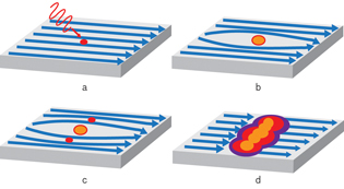 A photon is incident upon a nanowire (a) biased with a direct current near the critical current value, heating the nanowire and forming a localized hot spot (b) where the superconductivity is disrupted. The supercurrent diverts around this spot (c). For a sufficiently narrow wire (<100 nm), the local current density on either side of the hot spot exceeds the critical current density, causing a resistive region to span the entire cross section of the nanowire (d) and inducing a measurable voltage across the device.
The dimensions of a single wire segment are much smaller than the wavelength of light that must be detected, so even a diffraction-limited beam cannot be focused onto a very short wire. Thus, a nanowire is typically patterned to cover a larger area. Furthermore, the density with which wires are packed in this structure affects the absorptance of the detector, with a more tightly packed structure increasing the absorptance. Consequently, individual superconducting nanowire photodetectors typically have small active areas. They also cannot resolve the position, wavelength, or number of photons in an optical pulse, and require a minimum of several nanoseconds between detection events. Superconducting nanowire photodetector arrays, with their subwavelength gaps, address these shortcomings of individual nanowires and achieve a level of performance beyond that possible with a standard array configuration. Superconducting nanowire photodetector arrays also eliminate the need for complex optical coupling that is commonly necessary to increase the fill factor for other photon-counting array technologies.
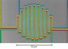 |
Each nanowire in a superconducting nanowire photodetector array (shown here in a false-color scanning electron microscopy image with four individual, spatially interleaved wires) can recover more quickly following a photon detection, and the other wires can be immediately available to detect subsequent photons. |
 |
A superconducting nanowire photodetector can be wrapped to cover a larger region of detection, but longer wires require greater recovery, or reset, time before detecting additional photons. |
Although a trade-off clearly exists in choosing nanowire length for a single detector (speed and yield improve for shorter nanowires while longer nanowires offer a larger coverage area for multimode signals), the superconducting nanowire photodetector array simultaneously combines many of the advantages of short and long nanowires.
One realization of a superconducting nanowire photodetector array utilizes a spatially interleaved array of four serpentine, superconducting nanowires that occupy a region 7 to 20 µm in diameter to form a single optical active area. In this case, each nanowire is four times shorter than would be needed if only a single nanowire had been used to cover the same total area. Therefore, each of the four shorter nanowires is faster and can be produced with higher yield, while the combination of elements covers a large area with tightly packed wires.
When illuminated by a single photon, only one of the interleaved nanowires registers a detection event. This single photon creates a hot spot that results in a large change in resistance, producing a signal that dominates all noise sources. The nanowire then quickly cools back down and the superconducting current is able to begin flowing in the nanowire again. The characteristic inductive time for the current in the detector to recover to its initial value depends on the length of the nanowire, and determines the reset time after a detection event before the next photon can be detected. However, during this time, the remaining nanowires are available to detect the next photon. This spatially multiplexed approach allows detection of photons at a higher rate than a single, superconducting nanowire would support, both because the individual nanowires are faster and because the array elements can count in parallel. Additionally, using multiple nanowires provides information about the number of photons in an optical pulse (up to the number of array elements) and permits the detection of photons separated by time periods much less than the reset time of a single nanowire.
One of the leading applications of this technology is in ultrahigh-sensitivity optical communication. The existing implementation of the superconducting nanowire photodetector arrays will permit photon-counting communication at faster rates than were previously possible. Whereas other existing near-infrared photon-counting detectors in the optical communication bands provide either high speed (e.g., photomultipliers) or high sensitivity (e.g., infrared avalanche photodiodes) alone, the Lincoln Laboratory superconducting nanowire photodetector arrays combine excellent performance in both sensitivity and speed.
"We're focused on really long-distance communication—lunar and planetary distances," Kerman explains. The superconducting nanowire photodetector technology will be used by Lincoln Laboratory for the NASA-funded Lunar Laser Communications Demonstration (LLCD). "The telecom industry isn't interested in such sensitive devices since they can send signals from amplifier to amplifier along the chain when they need it. We don't have the ability to put in an amplifier between here and the moon or Mars."
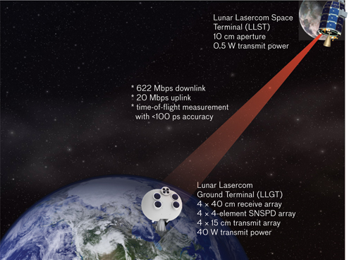 The Lunar Laser Communications Demonstration will demonstrate a long-distance, photon-counting, laser communication system capable of 622 Mbps optical downlink. The superconducting nanowire single-photon detector arrays will be used in the Lincoln Laboratory ground terminal.
 Past successful NASA space exploration missions have relied on radio-communication links to interplanetary spacecraft as well as to Earth-orbiting satellites. However, this modality will not support future missions that will deploy more sophisticated instruments (e.g., synthetic aperture radars) requiring data rates of much greater capacity. Optical networks represent the future of deep-space communications and will make it possible to collect ambitious data products from more distant destinations. Highly sensitive single-photon detection is a key enabler for this next generation of optical communication technologies.
Dr. Bryan Robinson, the lead system engineer on the LLCD program and a colleague of Dauler and Kerman, says that a probe used in a recent mission to Pluto with a 600 bit/s radio-frequency link will require approximately nine months to download the data collected during a few-week encounter with Pluto. Dauler responds, "A higher data rate communication system would enable more data collection. A mission's value and flexibility could be increased by near-real-time downloading of information."
The Lunar Laser Communications Demonstration rate of less than 6 × 10⁸ photons per second is still not pushing the detector to its limit.
The LLCD—part of the moon-orbiting Lunar Atmosphere and Dust Environment Explorer satellite experiment scheduled for launch in 2013—will demonstrate a long-distance, photon-counting, laser communication system capable of sending information at 622 Mbits/s from the moon to Earth. The superconducting nanowire photodetector arrays, located in a transportable ground terminal, will be key elements in this communication link. "The photon detection rate for this link is several hundred million photons per second," Dauler says. "This is still not pushing the detector to its limit."
The superconducting nanowire photodetector array has numerous intrinsic advantages—high performance in both sensitivity and speed, the largest photon-counting rates available, relative ease of fabrication, simple digital post-processing to obtain photon-number information, and precise photon timing information. These advantages make the technology adaptable to other potential applications:
- Single-photon-counting detectors for quantum key distribution systems demonstrated at 1.85 Mbits over 100 km distances—rates 100 times faster (for a fixed fiber-optical cable length) than previously reported.
- Ultrasensitive, time-resolved spectroscopy. Biological systems often exhibit fluorescence, which is sometimes in the infrared spectrum. For example, the singlet O2 fluorescence at 1.27 µm wavelength is important in cellular metabolic processes. Existing biological imaging systems focus on the visible domain because of the difficulty of working with long-wavelength imaging arrays. The availability of a high-speed, sensitive, infrared detector may enable new fundamental studies.
- Basic science experiments in quantum mechanics, including quantum imaging, quantum measurement, and quantum entanglement.
- A high-resolution, noncontact method to detect flaws in high-speed, very-large-scale integrated complementary metal-oxide semiconductor circuitry.
- Imaging technology. High-speed video imaging could be achieved with an array of nanowire photodetectors spread over the focal plane of an optical camera system.
top of page