A Little Light Work
Getting silicon to respond to light could usher in a new era of integrated optical devices.
Michael Geis stands in a cramped lab inside the Lincoln Laboratory complex, having borrowed half an hour on another researcher’s laser. Geis, a physicist in the Laboratory’s Submicrometer Technology group, needs this special laser to put one of his devices through its paces—devices that will perform optical functions in silicon that have long been limited to compound semiconductors such as gallium arsenide.
Already Geis and his colleagues have made an all-silicon photodetector that’s better at capturing light than any detector anyone else has built. But with researchers at labs from Intel to MIT to Cornell working on creating photonics components in silicon, it’s a bit of a horse race, the researchers say. The Lincoln Laboratory group is one of many research groups worldwide building highly integrated optical devices, analogous to integrated electronic devices made in silicon. Geis, Steven Spector, and Jung Yoon, physicists working on the project, are funded by the Defense Advanced Research Projects Agency (DARPA), which is promoting the development of such integrated silicon circuits.
Much digital data travels through fiber optics at the speed of light. Electronic data processing, however, is still stuck in the sand—or, more precisely, in silicon, the material in which cheap and powerful transistors are made. Scientists around the world are working to bring together the power of light—its speed, its lack of electrical interference—with the inexpensive and reliable processes that have made computer chips so successful. Such a technological blend could lead to electrooptic chips with the high performance and low cost of today’s complementary metal oxide semiconductor (CMOS) chips.
Geis, Spector, Yoon, and their colleagues in the Laboratory’s Submicrometer Technology group, along with Matthew Grein and Robert Schulein in the Optical Communications group, have made great strides in combining the two. In particular, they have built devices out of silicon that detect, filter, and modulate light waves—devices that previously could be made only out of other materials. The Lincoln Laboratory groups are collaborating with MIT electrical engineering professor Franz Kaertner’s group to show the Department of Defense they can build integrated circuits that can process optical signals. If they can make optical components out of silicon, instead of out of the compound semiconductors used in today’s lasers and photodetectors, they can easily integrate the components with the digital electronic devices built on silicon chips. Such a development would allow data to be ferried across chips not by metal conductors but by beams of light.
The trouble is that silicon and optics don’t mix well. At standard telecommunication wavelengths, from 1310 to 1550 nm, silicon is transparent. This quality can lead to good waveguides and filters but makes building devices such as detectors more difficult. In long-distance communications, compound semiconductors can bridge the gap between electronics and photonics, but devices made from these materials are too bulky and expensive to work on the scale of a chip.
The Lincoln Laboratory group has recently made a major step toward the fabrication of practical silicon photonics: they built a silicon-based photodiode sensitive at telecom wavelengths. To achieve this goal, they took advantage of the fact that defects in the atomic structure of silicon change how it interacts with light. “You go from something that is very transparent to something that is absorbing,” says Spector. Although this phenomenon has been known for 50 years, it has been mostly ignored for silicon because it was widely regarded as useless.
Their photodiode consists of a p-i-n waveguide (a strip of undoped, intrinsic silicon sandwiched between regions of n-type and p-type material) that is connected to aluminum conductors at its edges. Because light traveling along the waveguide changes how current flows through it, measuring current provides an indication of how much light is passing. The team discovered they could control the level of optical absorption by controlling the number of defects in the silicon. Their fabrication process uses standard doping techniques, implanting the silicon crystal with silicon ions. The interaction of silicon with silicon creates two kinds of defects—gaps, or vacancies, where an incoming atom knocks an already present atom out of place, and clusters where new atoms and dislocated atoms clump together. The researchers found that annealing the crystal resulted in cluster formation, which causes even greater sensitivity to light.
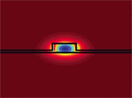 Most of the light in the silicon optical modulator passes through the center of the waveguide. “As you heat it up, these defects reassemble themselves,” Geis says. Above about 350°C, the silicon atoms move around and fill up the vacancies, so the gaps go away. But the other defects (the ones consisting of clusters of extra atoms) remain even when the material is heated to 475°C. Use of higher temperatures in fabricating the CMOS chips may eliminate these defects. However, Geis says that there is a dearth of information as to how well the defects would affect the absorption—or whether the changes they induced would stand up to the silicon manufacturing process. “We’re the first to see this defect because nobody ever did the experiment before,” Geis says. “Nobody thought it would work.”
The Lincoln Laboratory group is not the first to try doping silicon to get an optical response at telecom wavelengths. A team at McMaster University built a similar diode in 2003, but that device had much lower responsivity—too low to work as a practical photodetector. Geis and Spector improved on the earlier device by shrinking the waveguide tenfold (from roughly 5 μm across to about 0.5 μm) and by optimizing the defect implantation.
At 1550 nm, their device produces 0.8 amps of current per watt of optical input—roughly the same responsivity as the best commercially available high-frequency indium-gallium-arsenide photodiodes provide. The silicon devices also have lower leakage current, a measure of the electronic noise that reduces the amount of signal a device can handle: 0.2 nanoamps as compared to 1 to 50 nanoamps for commercial devices. The silicon device has a bandwidth of 10 to 20 GHz, which is considerable, but slower than the InGaAs device’s 50 GHz. If silicon photodetectors can be shown to be faster, as well as reliable and uniform, they may replace InGaAs photodiodes.
On the way to an all-silicon system, the Lincoln Laboratory team has been exploring devices that mix silicon and other materials, which they’ll use to build an integrated silicon photonic circuit. They have collaborated with MIT electrical engineering professor Judy Hoyt on a photodetector that combines silicon and germanium. Germanium is much better than silicon at detecting light in telecommunications systems because its bandgap corresponds perfectly to the 1550 nm wavelength light that optical fiber transmits best. But integrating germanium with silicon is difficult. For one thing, the crystal lattices of the two materials don’t match. Moreover, germanium deposition requires high temperatures during manufacturing, and the current devices produce more electrical noise than the InGaAs photodiodes. In the long run, fabrication simplicity favors an all-silicon process, but optimized germanium devices may offer better performance. Ultimately, the choice may depend on the application.
One device that will be essential for an integrated photonic circuit will be a silicon modulator to imprint a signal onto a light beam. The Lincoln Laboratory researchers, in collaboration with Kaertner’s group at MIT, designed a silicon modulator that’s very similar to their photodetector. The modulator is based on silicon waveguides in a standard Mach-Zehnder interferometer design. The waveguides split the beam in two, and an electrical charge alters the refractive index of one arm, so that when the beams merge again on the other side, they interfere to produce the signal. This design improves on a silicon modulator developed by Intel because it operates at only 0.02 volts per centimeter of the device’s length, whereas Intel’s uses about 16 volts per centimeter.
Achieving sufficient voltage in as short a length as possible is essential in shrinking the modulator onto a chip. The Lincoln Lab device got its better numbers by working in forward electrical bias, as opposed to Intel’s reverse bias. However, this approach causes the device to operate more slowly, a problem the researchers say they are working on. (Researchers at Cornell University have also demonstrated a design for a forward-bias device, offering different advantages and disadvantages from those of the Lincoln Laboratory approach.) In a related project, the Lincoln Lab team is developing tunable silicon filters to split different wavelengths of light into separate channels, allowing multiple signals to be sent simultaneously through a single fiber. Though such filters can be made with other materials—MIT electrical engineering professor Hank Smith, for example, is working on silicon-nitride filters—all-silicon filters offer a more direct path to a single-chip silicon system. The DARPA project requires the team to demonstrate a modulator, photodetector, and filter in a system by the end of the year.
That system won’t use all-silicon devices. It will, however, include the silicon-germanium detector and the silicon-nitride filters, which are further along in development. Still, the ultimate aim is to create an all-silicon circuit. Grein is leading the Laboratory’s effort to demonstrate an optically sampled analog-to-digital converter that uses these integrated optical components along with commercial devices.
The researchers are still trying to figure out the best ways to build the modulators and detectors, and are working through the trade-offs that optimizing any device entails. For instance, the photodiode is more sensitive when it’s bigger, absorbing about 99 percent of light when it’s 3 mm long. Increases in size produce more noise, of course, as well as lowering the frequency response. The researchers would like the photodiode to be only 0.25 mm long to fit on a chip, but such a small device length means less light absorption.
Spector says such device optimization will improve the performance of the modulator and detector by two- or threefold. The filters, he says, still need to be demonstrated. Although some engineering hiccups remain to be fixed in device fabrication, he’s optimistic that the problems will be worked out and that he and his colleagues will build an integrated device for processing optical signals. “The hope is to do it all in one chip,” he says, “and if the filters are there, we’ll be able to do it.” |