Detector Avoids Speed Traps
Material manipulation yields avalanche photodiodes sensitive at 1.9 to 2.5 μm.
How many layers of white paint do you need to cover a black wall? A single very thick coating will most likely do the job, but it may look streaky and uneven. A better question would be how many layers you need to change the black wall into a specific shade of gray. Now you need to proceed slowly with thin layers of white, and evaluate the results after each coating. Christine Wang, a materials scientist in Lincoln Laboratory’s Electrooptical Materials and Devices group, isn’t painting a black surface. Instead, she is tweaking crystalline layers to create her own version of a perfect gray—a series of lattice-mismatched buffer layers that transform a substrate lattice dimension into the base for a photodiode. And the result, if she succeeds, will be avalanche photodiode detectors (APD) for the short-wavelength infrared (SWIR) region from 1.9 to 2.5 μm. The major advantage of APDs over other infrared detectors is their greater sensitivity to light.
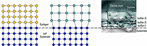 Materials whose lattices match the substrates can be deposited with no strain relief (left). Individual linear defects can accommodate the strain between slightly mismatched layers (middle). An electron micrograph shows a cross section of a series of mismatched layers (right). Note the strain relief and the absence of defects in the final buffer layer and the device layer. (The electron microscope image is from Wanlass et al., AIP Conf. Proc. No. 738, p. 427, 2004). Wang and her colleagues, Erik Duerr and Joseph Donnelly, designed, modeled, and tested the APDs to optimize the three-active-layer structure with high internal electric fields. Their aim was to ensure that the devices operate in Geiger mode—that is, past its breakdown voltage. In this mode, the detector delivers a large output signal even when struck by extremely low-intensity illumination. A photon hitting the active region of the APD generates an electron and a hole. Then the electric field drives the holes into a high-field multiplier layer, where impact ionization creates additional electron-hole pairs. The result is a cascade, or avalanche, of charge carriers. The high sensitivity of APDs makes them useful for photon counting or single-photon detection.
“The novelty of this work,” Wang explains, “is that we are working on extending the detection wavelength beyond conventional InP-based APDs.” Today’s best high-speed APDs are sensitive only to wavelengths shorter than 1.6 μm. But there is a wide window of atmospheric transmittance between 1.9 and 2.5 μm. Photon-counting detectors operating in this spectral region would allow low-light laser radar (ladar); they may also be useful in optical communications. In addition, chemical and biological agents have signatures in the SWIR. Wang says that while existing gallium-arsenide APDs already work in this region of the SWIR spectrum, those devices “suffer from very slow reset times”—that is, the time it takes between measurable signals. Since her devices, unlike the gallium-antimonide ones, appear to be free of the material defects that trap charge carriers, they exhibit reset times of tens of microseconds—nearly a thousand times faster than the GaSb-based APDs. Defects, which act as electron/hole traps, also affect the rates of detected “signals” when there is no actually input—the dark count. Wang’s materials have dark counts comparable to those of lattice-matched GaSb-based APDs.
A few years ago, Wang explains, Bernadette Johnson (leader of the Laboratory’s Biodefense Systems group) indicated that she was unable to locate any APDs that worked in the 2 to 2.5 μm region. Still, Johnson wasn’t sure of their potential usefulness. “If you don’t have it, you don’t know how effective it will be,” Wang says. However, she adds, “if we build it, they will use it.” Johnson is now actively interested in Wang’s results. She says that analysis of existing hyperspectral imaging data as well as measurements with extended InGaAs detectors “have identified some promising applications for sensitive imaging arrays” around 2 μm. Such applications, Johnson says, include “land mine detection, especially in vegetative ground cover, and bio-aerosol discrimination and classification.”
To fabricate their APDs, Wang and her associates need to alter the chemistry of the active layers so that the device responds at the appropriate wavelength. For example, in the formulation GaxIn1 – xAs lattice-matched to a substrate of InP, the detector’s wavelength of peak sensitivity changes from approximately 1.6 μm for high gallium concentrations to near 2.5 μm for high indium composition. But changing the chemical composition does more than tune the sensitivity wavelength. It also alters the distance between the atoms in the semiconductor crystal’s lattice, leading to a lattice mismatch between the active layer and the InP substrate. Somehow, the black wall of the substrate lattice dimension must morph into the gray of the active layer.
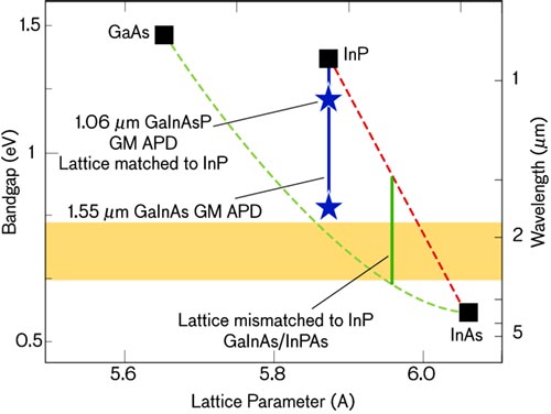
The orange band highlights the wavelengths of interest for III-V detectors. The blue vertical line indicates the series of materials that are lattice matched to an InP substrate. The green vertical line details the lattice and chemical information for Wang’s work. The red line linking InP to InAs shows the effect in both lattice parameter and wavelength of a chemical shift in the In(P, As) compounds. |
Lattice-mismatched detectors that work at the longer wavelengths require manipulating lattice chemistry to create designer substrates on which InGaAs/InPAs detectors reside. Wang does this manipulating by creating a series of buffer layers of In(PyAs1 – y) that build on an InP substrate, each with a slightly higher value of y as the phosphorous substitutes for the arsenic, until she achieves the proper lattice parameter base for the device layer, which has the formula (GaxIn1 – x) (PyAs1 – y). Wang’s associates Dan Calawa and David Chapman measure both the lattice parameters and chemical doping composition of the devices to confirm that their technique is working properly. Epitaxial growth is a slow process, in which layers are deposited one atomic layer at a time with a process called organometallic vapor-phase epitaxy (OMVPE). Wang must be careful to change the chemistry of each subsequent layer slowly. Otherwise, strain between mismatched layers will produce defects. It’s “painstaking work,” she says. “If you try to rush it, you have an inferior product.”
Wang must make one additional significant change. Her current work is based on nontraditional sources of arsenic and phosphorus sources: tertiary butyl arsine and tertiary butyl phosphine. Both are liquids. The industry standard OMVPE process, however, uses arsine and phosphine gases. “If we ever want this technology to be transferred to production,” she explains, “we have to go mainstream.” But following the standard process poses a potential difficulty. The liquids decompose at lower temperatures than arsine and phosphine gas. Wang is concerned that the higher temperature growth associated with arsine and phosphine gas may drive a faster deposition rate and, therefore, multiple starting points for layer growth. These islands of growth eventually connect with one another—but in doing so, create defects. Wang’s process, by contrast, lays down a complete monolayer before starting the next layer. In this way, she increases the probability of relieving interlayer strain while minimizing formation of defects. “We need to confirm that our growth kinetics still work with the new sources at the higher temperatures,” Wang concludes. When she makes her first full-scale 2.0 μm GaInAs/InPAs detector, using arsine/phosphine, that shows the same performance characteristics as her current material, her next question to Johnson and others might be: What wavelength do you want next? |