News
MIT Lincoln Laboratory receives five R&D 100 Awards
Five Lincoln Laboratory technologies were named 2010 recipients of R&D 100 Awards. These awards are given annually by R&D Magazine, an internationally respected journal providing news and technical articles to research scientists and engineers. Instituted in 1963, these awards recognize the 100 most technologically significant innovations introduced during the previous year. Recipients of R&D 100 Awards are chosen from hundreds of nominations by an independent panel of evaluators and the editors of R&D Magazine.
Previous R&D 100 award winners, which have included large companies, start-ups, universities, and government laboratories, span a broad range of applied research: fax machines, liquid crystal displays, antilock brakes, and the artificial retina.
The following innovations are the five winning Lincoln Laboratory technologies:- Geiger-Mode Avalanche Photodiode Detector Focal-Plane Arrays—a two-dimensional array of ultrasensitive solid-state photodetectors, each of which can measure the arrival time of single photons
- Subwavelength-Separated Superconducting Nanowire Single-Photon Detector Arrays—a component in an optical detection system that enables broadband single-photon detection with high efficiency and low noise at rates exceeding one billion photons per second
- Digital-Pixel Focal-Plane Array—a complementary metal-oxide semiconductor readout-integrated circuit for infrared imaging. Fast on-chip processing provides an extreme dynamic range from a minimally sized package.
- Runway Status Lights—a system integrating data from airport surveillance sources to control in-pavement lights that directly alert pilots to potential runway incursions
- Miniaturized Radio-Frequency Four-Channel Receiver—the smallest, least-power-demanding receiver that can detect frequencies over a six-octave range
The Geiger-Mode Avalanche Photodiode Array was developed by members of the ISR and Tactical Systems, Advanced Technology, and Aerospace divisions: Simon Verghese, Richard Marino, Brian F. Aull, Bernard B. Kosicki, Robert K. Reich, Bradley J. Felton, David C. Shaver, Eric A. Dauler, Pablo I. Hopman, Brian M. Tyrrell, Andrew H. Loomis, Douglas J. Young, K. Alexander McIntosh, David C. Chapman, Joseph P. Donnelly, Douglas C. Oakley, Antonio Napoleone, Erik K. Duerr, Jonathan P. Frechette, Peter J. Grossmann, Leonard J. Mahoney, Joseph M. Mahan, and Joseph E. Funk.
The primary application of this technology is as a detector array in a three-dimensional laser radar (ladar) camera. A three-dimensional ladar camera uses a very-short-pulse laser to illuminate an object and a Geiger-mode avalanche photodiode optical receiver that simultaneously images the reflected light and measures the time-of-flight of each photon, or distance, to each pixel in the image. The resulting data can be mapped so that color represents range in the image to produce a three-dimensional representation of the object.
Three-dimensional ladar cameras have been used to map terrain and construction sites, to acquire data for robotic vision, and to image partially obscured objects. The Geiger-mode avalanche photodiode focal-plane array is especially suited to these tasks because of its ability to detect and time-stamp single photons by using its unique, independent digital time-of-flight counting circuits, and its extremely high internal detector gain.
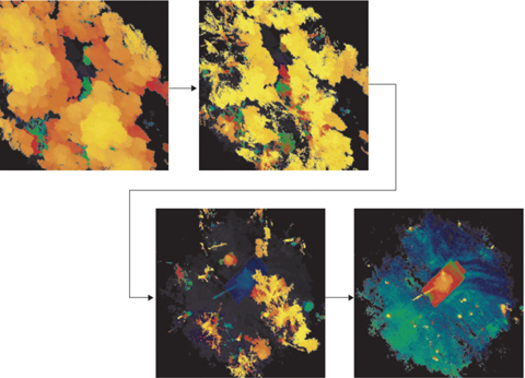 A sequence of three-dimensional images obtained by using a laser radar camera that includes the Geiger-mode avalanche photodiode focal-plane array can be processed and registered to remove foliage that obscures objects of interest below. In the four images, color represents relative height. By changing the threshold and eliminating taller objects from view, the upper left image showing only treetops progresses to the lower right image revealing a tank and tree trunks. A sequence of three-dimensional images obtained by using a laser radar camera that includes the Geiger-mode avalanche photodiode focal-plane array can be processed and registered to remove foliage that obscures objects of interest below. In the four images, color represents relative height. By changing the threshold and eliminating taller objects from view, the upper left image showing only treetops progresses to the lower right image revealing a tank and tree trunks. |
The Subwavelength-Separated Superconducting Nanowire Single-Photon Detector Array was developed through a collaboration with MIT Research Laboratory for Electronics. Its inventors are Eric A. Dauler and Andrew J. Kerman of Lincoln Laboratory's Optical Communications Technology Group, Karl K. Berggren, a professor at MIT, and Vikas Anant and Joel K.W. Yang, both former graduate students at MIT. The superconducting nanowire detector array was designed to enable the next generation of optical communication technologies, which demand large-capacity data rates. The nanowire photodetector array’s primary function is to rapidly detect individual photons.
The array dramatically improves the performance and capability of standard single nanowire photodetectors, which cannot resolve the position or wavelength of detected photons and can detect, at most, one photon at a time with a minimum time period of several nanoseconds between detection events. By using a spatially interleaved array of up to eight serpentine, superconducting nanowires that occupy a region 7 to 20 micrometers in diameter, nanowire photodetector arrays overcome those limitations of the single nanowire. "Multiplexing the detectors permits a much higher detection rate—more than one billion photons per second—than a single nanowire detector can achieve," technical staff member Eric Dauler explains. "Plus, our method doesn't require complex optical coupling techniques common in other photon-counting arrays."
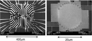 (Left) A scanning electron micrograph of two 8-element nanowire photodetector arrays fabricated at Lincoln Laboratory. (Right) A magnified scanning electron micrograph of a single 8-element nanowire array. (Left) A scanning electron micrograph of two 8-element nanowire photodetector arrays fabricated at Lincoln Laboratory. (Right) A magnified scanning electron micrograph of a single 8-element nanowire array. |
The nanowire photodetector arrays were also chosen for the 2009 Lincoln Laboratory Best Invention Award, which recognizes the most significant new device, method, or process, developed from study or experimentation, that resulted in a filed technology disclosure, patent application, or patent license within the previous two years.
An analog-to-digital converter in every pixelThe Digital-Pixel Focal-Plane Array was developed by a multidivisional team including Michael W. Kelly, Kenneth I. Schultz, Lawrence M. Candell, Daniel L. Mooney, Curtis B. Colonero, Robert Berger, Brian M. Tyrrell, James R. Wey, Christopher L. David, Stephanie Hsu, Andrew M. Siegel, Joseph S. Costa, Eric J. Ringdahl, Matthew G. Brown, Justin J. Baker, and Thomas D. Gardner.
The Lincoln Laboratory digital-pixel focal-plane array is designed to meet demands of emerging infrared imaging applications, such as day/night persistent surveillance, aerial search and rescue, and environmental remote sensing. These applications require high-sensitivity, high-resolution, large-field-of-view, and fast-data-rate imaging.
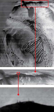 Aerial infrared image of Mount Washington, N.H., on a winter morning. The size of the large image is approximately 200 megapixels. This infrared image has about 10 times the information of a high-definition television image. The image insets culminate with the silhouette of the Mount Washington Observatory at the summit of Mount Washington.
This novel focal-plane array includes a low-power analog-to-digital converter in every pixel and enables greater computational capability. The digital-pixel focal-plane array combines a commercial sensor with a Lincoln Laboratory–designed readout integrated circuit that leverages advanced semiconductor processes to enable low-power, high-component-density designs. It can function as a conventional imager; however, its architecture also provides a simple way to implement real-time image processing algorithms on chip prior to reading out the data.
"The in-pixel digitization feature of this focal-plane array enables on-chip data processing, an extremely large dynamic range, and a fast data readout rate. These capabilities further enable imaging feats that are impossible with other current technologies," says assistant group leader Michael Kelly.
The significant improvements over conventional approaches in effective detector operability, dynamic range, area-coverage rate, high digital-data rates, and size, weight, and power requirements permit the digital-pixel focal-plane array to outperform other focal-plane arrays in existing imaging applications (e.g., very-wide-area, high-resolution, high-sensitivity, persistent surveillance) and also to be utilized for new applications (e.g., weather forecasting, industrial monitoring).
The digital-pixel focal-plane array has been demonstrated with various detector technologies, is being used to assess new long-wave infrared detector technologies, and has been selected by the U.S Army for future infrared systems.
Providing safety information directly to pilotsA team including James R. Eggert, Eric M. Shank, Walter L. Brown, Richard W. Bush, Jeffrey L. Gertz, Leo Javits, Daniel A. Komisar, Maria Picardi Kuffner, Jessica E. Olszta, and Harald Wilhelmsen of the Surveillance Systems Group and Daniel C. Herring of the Embedded and High Performance Computing Group developed the Runway Status Lights system for the Federal Aviation Administration (FAA). The system alerts pilots when a runway is unsafe by turning on special red lights, embedded in the runway pavement, that are fully visible to pilots and nearby personnel. The lights are controlled by safety logic that automatically processes surveillance information from a preexisting surveillance system. The system serves as an independent backup to the clearances broadcast by air traffic controllers, issuing alerts rapidly to all aircraft approaching an intersection at which a collision may be imminent.
 Takeoff Hold Lights are shown implemented at the Los Angeles International Airport. These components of the Runway Status Lights system are placed at departure positions and indicate to pilots that it is unsafe to take off because a runway ahead is occupied by another aircraft.
Preventing runway incursions that may lead to runway accidents has been on the National Transportation Safety Board's "Most Wanted List" for over a decade. Studies of runway incursions that occurred between 1997 and 2000 at 100 of the busiest airports found that the status lights system might have prevented or mitigated 75% of the 1667 identified incursions. In 2007, the FAA announced it will install Runway Status Lights at 22 major airports in the U.S. National Airspace System by 2011.
More sensitive detection for constrained platformsThe Miniaturized Radio-Frequency Four-Channel Receiver was developed by Helen H. Kim, Matthew D. Cross, Merlin R. Green, Daniel D. Santiago, and Sabino Pietrangelo of the Advanced RF Sensing and Exploitation Group in the ISR and Tactical Systems Division. This radio-frequency (RF) receiver, formed from a single chip set, is considerably smaller, has greater sensitivity, and demands significantly less power than existing commercial RF systems. The system demonstrates the largest measured spur-free dynamic range (an indicator of how well a target signal can be distinguished from interference) for an RF receiver of any size. With dimensions about the same as a standard six-inch school ruler, the miniaturized receiver is suitable for military and commercial applications that have only a small platform on which to fit an RF sensor system consisting of antennas, receivers, signal processors, and data links.
To put the capability of this RF receiver in context, Helen Kim, one of the technology's developers, says, "Compare a cell phone from the 1990s to one of today's tiny smart phones. By leveraging the same technological advances in consumer electronics and adding new circuit techniques, we have miniaturized radio-frequency receivers while increasing performance."
The miniaturized RF receiver, which leverages improvements in commercial silicon germanium semiconductors, detects low-level signals of interest. Signals of interest cover a very broad range of frequencies, may be very weak, and may be obscured by large interfering signals, such as those emitted by television or radio stations. The miniature receiver's sensitivity makes it adaptable for radar and communications applications that must operate in environments of complex interference.
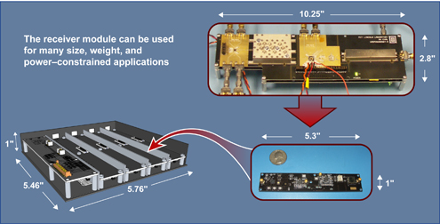 The components of a miniaturized RF receiver module are packaged on a
 1-inch × 5.3-inch board. The four-channel receiver occupies only one 6U VME card and has a size of 5 × 5 × 1 cubic inches. For comparison, a commercial two-channel RF receiver uses four 6U VME cards and has a size of 5 × 9 × 1.6 cubic inches.
Lincoln Laboratory previously received R&D 100 Awards in 1995 for Global Positioning System (GPS)-Squitter technology, a technique for automatic dependent surveillance of aircraft by broadcasting GPS position data, and in 1998 jointly with Cyra Technologies and the Los Alamos National Laboratory for the Cyrax Portable, 3D Laser-Mapping and Imaging System.
Posted August 2010